thanks for watching reading enjoy!
[PR]上記の広告は3ヶ月以上新規記事投稿のないブログに表示されています。新しい記事を書く事で広告が消えます。
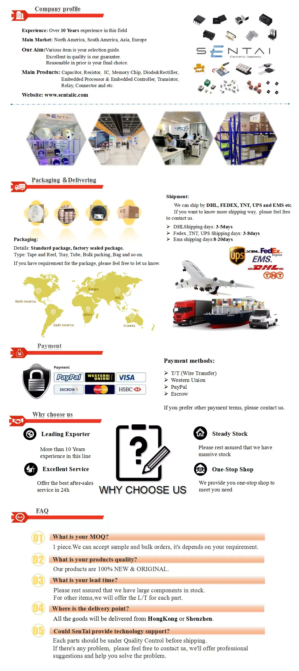
One-stop Service:
1.Competitive Price (Factory direct price).
Welcome here and I will try my best to satisfy you well
with competitive prices as per you r request.
2. On time delivery.
3. Good customers service.
4. Professional Technology.
5. Quality Control through the whole Manufacturing process.
All products have to pass strict inspection before they go out.
We believe that quality is the soul of an enterprise.
6. Flexibility
Customers-oriented. We forever center on customers' demands
constantly update and introduce into technology
fully understand customers' requirements and offers our professional suggestion.
|
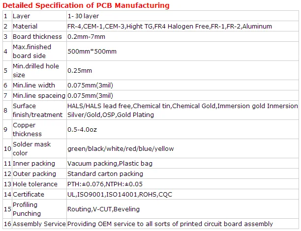
NO |
Items |
Technical Capabilities |
|
1 |
PCB and Layers |
Rigid PCB, Rigid-Flex PCB, 1-20 layers |
|
2 |
Materials |
FR4, FR5, High Tg, CEM3, Rogers, Aluminum Base, PET Material |
|
3 |
Surface |
Lead-Free Hal, HAL, Flash Gold, Immersion Gold , Immersion Tin, Immersion Silver, Gold Fingers, OSP, Impedance Control |
|
Four |
Max Board Size |
450 mm x 1200 mm |
|
Five |
Min Board Thickness |
4 Layers: 0.4 mm (16 mil) 6 Layers: 0.8 mm (32 mils) 8 Layers: 1.2 mm (48 mil) 10 Layers: 1.6 mm (64 mil) |
|
6 |
Min Line Width |
0.10 mm (4 mil) |
|
7 |
Min Line Spacing |
0.10 mm (4 mil) |
|
8 |
Min Hole Size |
0.20 mm (8 mil) (Also Blind / Buried holes) |
|
9 |
PTH Hole Size Tolerance |
± 0.076 mm (± 3 mil) |
|
Ten |
NPTH Hole Size Tolerance |
± 0.05 mm (± 2 mil) |
|
11 |
Hole Position Tolerance |
± 0.05 mm (± 2 mil) |
|
12 |
Min S / M Pitch |
0.10 mm (4 mil) |
|
13 |
Twist and Bent |
≤ 0.75% |
|
14 |
Aspect Ratio |
12: 1 |
|
15 |
Electric Strength |
≥ 30 KV / mm |
|
16 |
Peel strength |
≥ 1.4 N / mm |
|
17 |
Solder Mask Abrasion |
≥ 6 H |
|
18 |
Thermal Stress |
288 ° C / 20 Sec. |
|
19 |
Flammability |
94V—0 |
|
20 |
Test Voltage |
50-300 V |
We have massive components in stock
You Have More If RFQ, Please Feel Free To Contact Us.
We Will Offer The Best Price For You Learn More About MOKOTek Tracker !
1. OEM&ODM electronic PCB/PCBA design and engineer.
2. HASL/ENIG/OSP surface finishing technology.
3. DIP/SMT/SMD component assembling.
4. AOI,ICT,Function Testing methods.
5. UL,RoHS, SGS, ISO9001, ISO14001 approved.
6. 2 years warranty, we protect your legal interest even we are in different countries.
We make particular specification PCB/PCBA as you want ,please send us the Gerber file and BOM list for a quotation.(Your confidential Documentations&Intellectual Properties are under our protection!)
Your Trust Makes It A Great Honor For Our Team To Serve For Your Interest! We Take Your Opinion Seriously.
One Piece Order Accepted. Contact Us FOR MORE INFORMATION(Click to Visit Our Frontpage)

Founded in the year 2001,located in Shenzhen, as a professional OEM/ODM Manufacturer, MOKO is born to produce high quality product,provide the best engineer service,serve for our customers' core interests.We could provide one-stop pcb assembly service,we also offer:
- Contract Manufacturing
- Engineering Services
- PCB Design & Assembly
- Component Procurement & Material Management
- Product Design
- Fast Track Prototyping
- Cable and Wire Assemblies
- Plastics and Molds
- Function Testing Service
Technical requirement:
1) Professional Surface-mounting and Through-hole soldering Technology check the LOrawan project https://mokotek.com/lw001-bg-lorawan-tm-gps-tracker/
2) Various sizes like 1206,0805,0603 components SMT technology
3) ICT(In Circuit Test),FCT(Functional Circuit Test) technology.
4) PCB Assembly With UL,CE,FCC,Rohs Approval
5) Nitrogen gas reflow soldering technology for SMT.
6) High Standard SMT&Solder Assembly Line
7) High density interconnected board placement technology capacity.
Quote requirement:
· Gerber file https://circuitpeople.com/Blog/WhatIsAGerberFile.aspx of the bare PCB board
· BOM (Bill of material) for assembly
· To short the lead time, please kindly advise us if there is any acceptable components substitution.
· Testing Guide & Test Fixtures if necessary
· Programming files & Programming tool if necessary
· Schematic if necessary
Advanced PCB assembly Equipment:
· SMT Machine: SIEMENS SIPLACE D1/D2 / SIEMENS SIPLACE S20/F4
· Reflow Oven: FolunGwin FL-RX860
· Wave Soldering Machine: FolunGwin ADS300
· Automated Optical Inspection (AOI): Aleader ALD-H-350B
· Fully-Automatic SMT Stencil Printer: FolunGwin Win-5
 PCB Leadtime:
| Single/double side | 4 layer | 6 layer | Above 8 layer | HDI | |
| Sample lead time(Normal) | 5-6 | 6-7 | 7-8 | 10-12 | 15-20 |
| Sample lead time(Fastest) | 48-72 hours | 5 | 6 | 6-7 | 12 |
| Mass production lead time(First batch) | 7-9 | 10-12 | 13-15 | 16 | 20 |
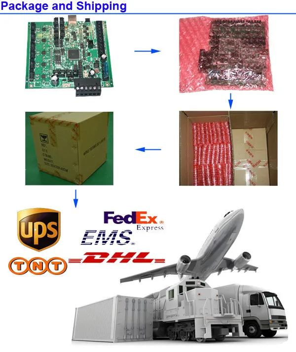
Shipping Methods
1.By DHL, UPS, FedEx, TNT using clients account.
2.By EMS (Usually for Russia Clients), but the price is high.
3.By sea for mass quantity according to customer's requirement.
4.By customer's Forwarder
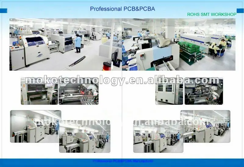
1)RoHS SMT Processing:
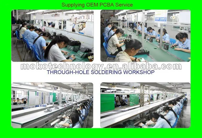
2)High Standard Through-Hole Components Soldering Workshop
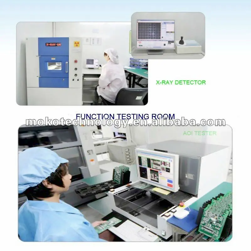
3) Full Equipped Function Circuit Testing Room
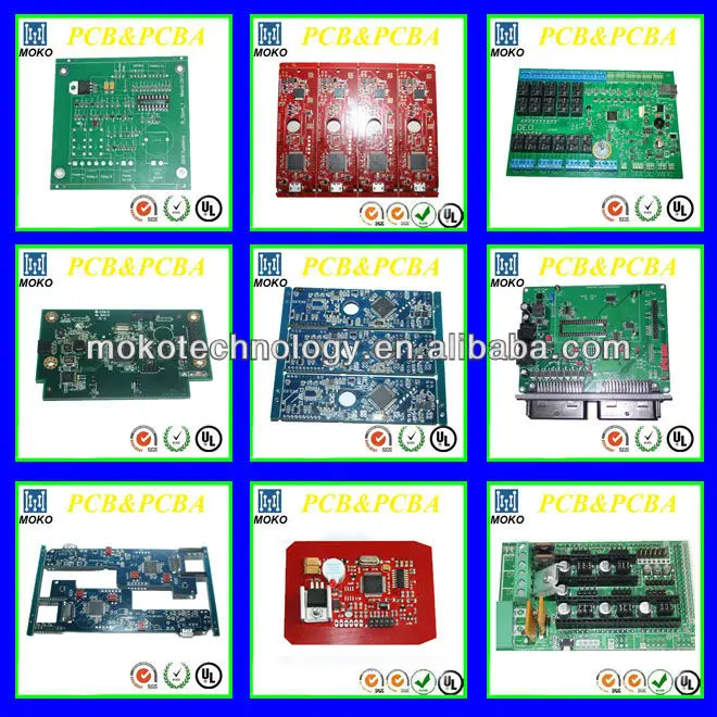
PCBA Products Showcase
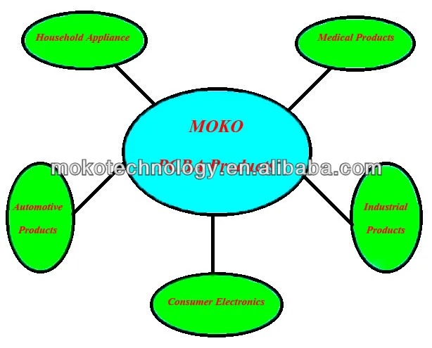
Products Application

Q:What's files do you use in the bare board fabrication?
A:Gerber RS-274X,274D,Eagle and AutoCAD's DXF,DWG
Q:What's files do you need in the PCBA projects?
A:Besides the pcb file, the PNP(Pick and Place) file and Components Position file are also needed.
Q: How can I know the processing about my PCB or PCBA order?
A: Each Customer has a sale manager to contact with you. MOKO working hours:AM9:00-PM6:00(Beijing Time) from Monday to Friday. We will reply your email in 2 hours in our working time. And you also can contact with our sales's cell phone if urgent.
Q: Will our product be tested before shipment?
A: Yes, we could provide Function Circuit Testing if you provide us the testing methods.